Nanoscale heterostructures have attracted more and more attention in recent years owing to the multifunctional and integrated request for the nanodevices[1]. A great deal of effort has been put in the synthesis of nanoscale heterostructures with controllable composition and properties,such as the superlattices,nanocables and hierarchical nanostructures[2]. The interface between two different materials is very important for a heterostructure,because it will greatly influence the performance of the devices based on such heterostructures[3,4,5]. Epitaxial growth is an effect technique to obtain the perfect interface in the heterostructures[6,7].However,the epitaxial growth generally occured between the materials with the same crystal structures,such as Si/Ge and GaAs/InAs.
Both SnO2 and ZnO have been intensively studied due to their outstanding properties and potential applications in nanoscale electronics,optics,sensors and other novel devices[8,9,10,11,12]. Recently,the disordered heterostructures composed of ZnO and SnO2,such as the side-to-side SnO2/ZnO/SnO2 triaxial nanobelt and the core-shell ZnO/SnO2 nanostructures,have been reported[13,14]. However,it is still a big challenge to prepare the epitaxial growth ZnO-SnO2 heterostructures due to the quite different crystal structures of these two materials. SnO2 belongs to the Rutile structure with the lattice constants a=0.4737 nm and c=0.3186 nm,but ZnO has a wurtzite structure with the lattice constants a=0.3249 nm and c= 0.5206 nm. Meanwhile,it is not difficult to find that the atomic stacking is similar in some crystal planes of SnO2 and ZnO. For example,in the wurtzite ZnO crystal,the atomic stacking along the c axis is the hexagonal closest packing,which is similar for the rutile SnO2 crystal along the a axis.Such structure similarity makes it possible to epitaxial grow the SnO2 -ZnO heterostructures,which was proved by a recent report[15]. However,the two-step process used two different methods,thermal evaporation and the hydrothermal method,make the synthesis process complicated. In addition,it was found that the ZnO seeds are indispensable for the formation of the SnO2-ZnO epitaxial heterostructures. In this study,we used a simple and fast,two-step thermal evaporation process to synthesize the SnO2-ZnO epitaxial heterostructures. The ZnO nanrods were directly epitaxial grown on the SnO2 backbones without using the ZnO seeds. The SnO2-ZnO heterostructures exhibited good photocatalytic performance for the organic dyes degradation. 1 Experimental Section 1.1 Synthesis of ZnO-SnO2 nanodendrites
The experiments were carried out in a tube furnace via a two-step thermal evaporation method. First,pure Sn powder was placed at the center of the tube,and several alumina plates served as the substrates were placed at 10 cm downstream. After evacuated,50 sccm Ar and 5 sccm O2 was introduced into the furnace and kept the vapor pressure at 5 torr. Then the furnace was heated to 850 ℃ and kept for 90 min. After cooled to room temperature,the product of the first step was taken out and used as the substrates for the next step to grow ZnO. The second step of the ZnO growth is a typical method according to the previous report[16]. After the two-step process,products on the substrates were collected for further characterization. The structures of the products were checked by X-ray diffraction (XRD,M18AHF). The morphologies and microstructure of the products were investigated by scanning electron microscopy (SEM,Hitachi S-4300) and high resolution transmission electron microscopy (HRTEM,JMS 2011). 1.2 Photocatalytic experiments
The photocatalytic experiments were performed under the illumination of a high pressure mercury lamp. The alumina substrate (20×5 mm) with the as-prepared ZnO-SnO2 nanodendrites was immersed in 50 mL aqueous solution of methyl orange with a concentration of 5 mg/L. Absorbance spectrum was monitored every 20 min. 2 Results and Discussion
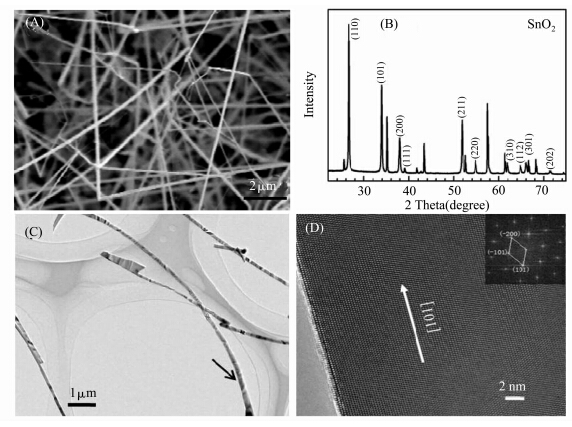
The first product studied was obtained in the first thermal evaporation step. The SEM image shown in Figure 1A reveals that the products are large quantities of nanowires. The nanowires are several tens of micrometers in length and 80—120 nm in diameter. Figure 1B shows the XRD patterns recorded from the sample shown in Figure 1A. Most of the diffraction peaks can be indexed to the tetragonal SnO2(JCPDS No. 88-0287),and the unlabelled peaks are attributed to the Al2O2 substrate. Figure 1C and 1D are the typical TEM and HRTEM images of the nanowire. The distances between the clear lattice fringes are 0.26 nm and 0.24 nm,corresponding to the (-101) and (-200) planes of the tetragonal SnO2,respectively. According to the HRTEM results and the FET image,it can be deduced that the SnO2 nanowires are single crystal and grow along the [101] direction.
 | Figure 1 (A) SEM image of the SnO2 nanowires synthesized at the first step; (B) XRD pattern of the nanowires; (C) TEM image of the nanowires; (D) HRTEM image and the corresponding FET image(inset) taken from an individual nanowire |
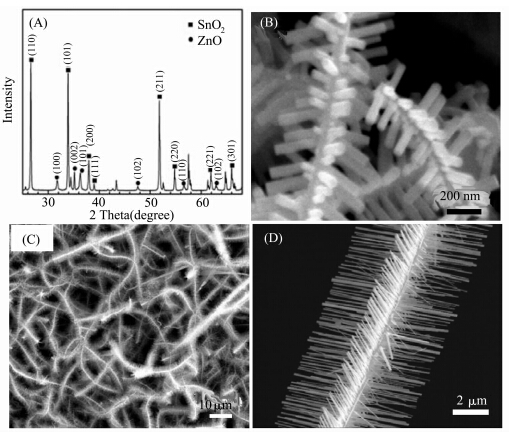
Figure 2 shows the morphology and structure analysis of the products obtained in the second step. The XRD results (Figure 2A) confirmed that two different phases,i.e. the tetragonal SnO2 (JCPDS No. 88-0287) and the hexagonal ZnO (JCPDS No. 36-1451),co-exist in the product. The SEM observation reveals that a hierarchical nanostructure was formed in this step,as shown in Figure 2B,2C and 2D. The hierarchical structure is composed of the SnO2 nanowire backbone and the numerous ZnO nanorods assembled on the SnO2 nanowire. The length and diameter of the ZnO nanorods could be controlled by adjusting the duration of the second step. Figures 2B is the SEM image of the as-synthesized products with growth duration of 30 min. After 30 min growth,the central axial SnO2 nanowires are surrounded by radial oriented nanorods with diameter of about 20 nm and length of about 200 nm. When the ZnO growth time was prolonged to 60 min,as shown in Figure 2C and 2D,the branches evolved from nanorods to nanowires with size of about 50 nm in diameter and 2 μm in length. The branch nanowires were radially grown on the SnO2 nanowire with a 4-row symmetrical ordered assembly.
 | Figure 2 (A) XRD pattern of products synthesized at the second step; SEM images of the sample with growth duration of (B) 30 min and (C),(D) 60 min,respectively |
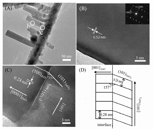
The morphology and structure of the nanodendrites were further characterized by TEM. A representative TEM image of the nanostructure is shown in Figure 3A. A clear interface can be found between the SnO2 backbone and the ZnO nanorod branches. The microstructure of the ZnO-SnO2 heterostructure was studied by HRTEM recorded from different locations. Figures 3B and 3C show the lattice-resolved HRTEM images taken from the sites b and c marked in Figure 3A,respectively. In Figure 3B,the fringe spacing is 0.52 nm,corresponding to the identify distance of the (001) plane in wurtzite ZnO. The SAED pattern (inset of Figure 3B) is accordance with the HRTEM analysis. These results demonstrate that the branch nanorod is single-crystalline ZnO with a growth direction of [001]. The HRTEM image taken from the interface region around the branch nanorod and the backbone nanowire is shown in Figure 3C. It was found that the interface is parallel to the (001) plane of the branch ZnO and the growth direction of SnO2. The ZnO and SnO2 have a crystalline orientation relationship as follows: [010]ZnO//[010]SnO2,(001)ZnO//(-101)SnO2. And the angle between the growth plane of ZnO(100) and SnO2 (101) is about 157°. Figure 3D is the schematic model of the interface region of the heterojunction. Along the boundary,the lattice constants of the ZnO (100) and SnO2 (101) are 0.28 nm and 0.26 nm,respectively. There is an angle of 157° between these two planes That deflection could avoid the lattice mismatch of about 5.6% between the ZnO (001) and SnO2 (101) and ensure the epitaxially growth of the ZnO (001) plane from the SnO2 (-101). Actually,the planes of the ±(-101) and symmetrical ±(101) of the SnO2 were exposed during formation of SnO2 nanowires[17] and served as active planes to provided preferable sites for ZnO deposition when the ZnO vapor arrived in second step. As a result,the hierarchical nanostructure consisted of 4-rows of secondary ZnO wires grown from ± (-101) and ±(101) planes of SnO2 trunk is formed.
 | Figure 3 (A) Typical TEM image of single nanodendrite; (B),(C) HRTEM images taken from location b and c marked in Fig. 3A,respectively; (D) A schematic diagram of the heterojunction interface showing the epitaxial and orientation relation |
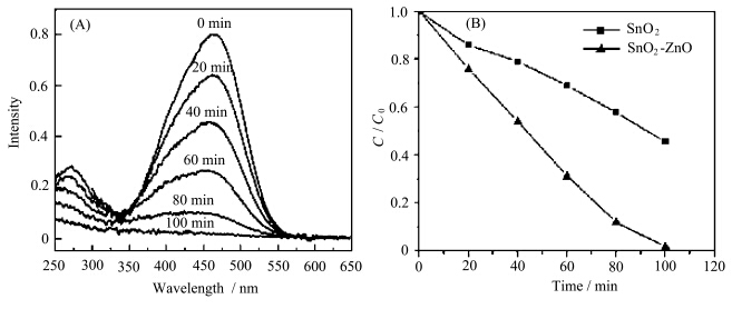
It is reported that the SnO2-ZnO compound semiconductor is an effective system for the photocatalytic applications. However,it is likely to form some defects at the interfaces of the two semiconductors,which will become the recombination centers for the photo-induced carriers. The epitaxial relationship between the ZnO and SnO2 nanowires in the present heterostructures can eliminate this drawback. Combing the large surface areas provided by dendritic morphology,the hierarchical ZnO-SnO2 nanostructure should be a good candidate for photocatalyst. The photocatalytic property of the as-synthesized ZnO-SnO2 nanostructure was investigated by the photodegradation of methyl orange. Figure 4A shows the UV-Vis absorption spectra of the methyl orange solution after illuminated for different durations. With increasing the irradiating time,the absorption of methyl orange weakened,which means that the concentration of the methyl orange decreased. After 100 min irradiation,the methyl orange was almost totally decomposed. A comparative experiment was done to the pure SnO2 nanowires under the same condition,which results are shown in Figure 4B. It can be seen that the SnO2-ZnO heterostructures exhibited a much better photocatalytic performance than that of the SnO2 nanowires. Two possible reasons might be responsible for the enhanced performance. First,the SnO2-ZnO heterojunction can enhance the photocatalytic capability by increasing the efficiency of the charge separation and restricting the recombination of the photo-induced carriers. Second,ZnO also has photocatalytic activity under the UV light illumination.
 | Figure 4 (A) UV-Vis absorption spectra of methyl orange solution,the original solution with 5 mg/mol in concentration was treated by the nanodendrites sample for 0,20,40,60,80,100 min; (B) Degradation rate versus time over two samples (with and without the nanodendrites catalyst) |
In summary,ZnO-SnO2 nanodendrites were synthesized via a two-step thermal evaporation process. High oriented 4-rows of the ZnO branches were hetero-epitaxial grown on the SnO2 trunks. Present ZnO-SnO2 nanodendrites displayed an evident capability of the photocatalytic decomposition to methyl orange. The heterojunction with special hierarchical structure provide a potential application for photocatalytic degradation of organic pollutants in sewage and air.
AcknowledgementsThis work was supported by Chinese Academy of Sciences,NSFC (Grant Nos. 21103211,51272258,51272302,50902134,and 61025003) and National Basic Research Program of China (973 Program) (Grant Nos. 2010CB934103 and 2012CB932400).
| [1] | Hillerich K, Dick K A, Wen C Y, et al. Strategies to control morphology in hybrid group Ⅲ-Ⅴ/group Ⅳ heterostructure nanowires [J]. Nano Letters, 2013, 13(3): 903-908. |
| [2] | Takei K, Madsen M, Fang H, et al. Nanoscale InGaSb heterostructure membranes on Si substrates for high hole mobility transistors [J]. Nano Letters, 2012, 12(4): 2060-2066. |
| [3] | Stephen A, Dunn G M, Oxley C H, et al. Improvements in thermionic cooling through engineering of the heterostructure interface using Monte Carlo simulations [J]. Journal of Applied Physics, 2013, 114(4): 043717. |
| [4] | Zhang M, Kong Y C, Zhou J J, et al. Polarization and interface charge coupling in ferroelectric/AlGaN/GaN heterostructure [J]. Applied Physics Letters, 2012, 100(11): 112902. |
| [5] | Gadre M J, Lee Y L, Morgan D. Cation interdiffusion model for enhanced oxygen kinetics at oxide heterostructure interfaces [J]. Physical Chemistry Chemical Physics, 2012, 14(8): 2606-2616. |
| [6] | Sun H D, Woodward J, Yin J, et al. Development of AlGaN-based graded-index-separate-confinement-heterostructure deep UV emitters by molecular beam epitaxy [J]. Journal of Vacuum Science and Technology, 2013, 31(3): 03C117. |
| [7] | Hudait M K, Zhu Y, Johnston S W, et al. Ultra-high frequency photoconductivity decay in GaAs/Ge/GaAs double heterostructure grown by molecular beam epitaxy [J]. Applied Physics Letters, 2013, 102(9):093119. |
| [8] | Konenkamp R, Word R C, Godinez M. Ultraviolet electroluminescence from ZnO/polymer heterojunction light-emitting diodes [J]. Nano Letters, 2005, 5(10): 2005-2008. |
| [9] | Cheng Y, Xiong P, Yun C S, et al. Mechanism and optimization of pH sensing using SnO2 nanobelt field effect transistors [J]. Nano Letters, 2008, 8(12): 4179-4184. |
| [10] | Zhao M G, Li Z L, Han Z Q, et al. Synthesis of mesoporous multiwall ZnO nanotubes by replicating silk and application for enzymatic biosensor [J]. Biosensors and Bioelectronics, 2013, 49: 318-322. |
| [11] | Wang Z L. Zinc oxide nanostructures: growth, properties and applications [J]. Journal of Physics: Condensed Matter, 2004, 16: R829. |
| [12] | Kuang Q, Lao C S, Wang Z L, et al. High-sensitivity humidity sensor based on a single SnO2 nanowire [J]. Journal of the American Chemical Society, 2007, 129(19): 6070-6071. |
| [13] | Zhao J W, Ye C H, Fang X S, et al. Selective growth of crystalline SnO2 on the polar surface of ZnO nanobelts [J]. Journal of Crystal Growth, 2006, 6(12): 2643-2647. |
| [14] | Yu W D, Li X M, Gao X D. Microstructure and photoluminescence properties of bulk-quantity SnO2 nanowires coated with ZnO nanocrystals [J]. Nanotechnology, 2005, 16: 2770-2774. |
| [15] | Cheng C W, Liu B, Yang H Y, et al. Hierarchical assembly of ZnO nanostructures on SnO2 backbone nanowires: low-temperature hydrothermal preparation and optical properties [J]. ACS Nano, 2009, 3(10): 3069-3076. |
| [16] | Wang X D, Ding Y, Summers C J, et al. Large-scale synthesis of six-nanometer-wide ZnO nanobelts [J]. The Journal of Physical Chemistry B, 2004, 108(26): 8773-8777. |
| [17] | Wang J X, Liu D F, Yan X Q, et al. Growth of SnO2 nanowires with uniform branched structures [J]. Solid State Communications, 2004, 130: 89-94. |


