


随着社会的发展,伴随而来的环境问题引起了人们越来越广泛的关注,因此发展廉价、高效的光催化剂来降解工业产出、起居生活等方面带来的有机污染物成为许多研究领域的热点。一些纳米材料在新能源的利用,以及污染物的降解方面具有广阔的应用前景[1, 2],如α-Fe2O3[3]、Cu2O[4]、CdS[5]、CdSe[6]、TiO2[7]等,以其独特的结构和物理化学性质被广泛应用于光催化领域,如水的裂解、有机污染的光降解等[8,9,10]。但是,以上提到的这些材料在应用方面还存在着很多问题,如Cu2O 和α-Fe2O3[11]的光催化效率已达到瓶颈,很难大幅提高,而CdS 和CdSe 具有很强的毒性,对环境有很大的污染。因此,研究人员将目光转移到了环境友好、高效的新型催化材料上。
硅是一种储量丰富、绿色环保的材料,特别是SiNWs由于其独特的物理化学性质引起了许多科学工作者的兴趣[12, 13]。SiNWs的能带介于1.1~3.5 eV 之间,并且可以通过调控SiNWs的直径改变其禁带宽度[14]。同时,SiNWs是直接带隙半导体,其能带宽度对可见光的波长范围具有很好的匹配度,因此SiNWs在光催化领域有很好的应用前景[15,16,17,18]。至今为止,已经有多种方法用于制备SiNWs,例如化学刻蚀法、激光剥蚀法、分子束外延法等[19]。但是,刻蚀法制备的SiNWs表面存在大量的晶格缺陷,导致许多载流子运输过程中被缺陷捕获,从而降低了其催化效率,大大阻碍了SiNWs在光催化方面的应用[20, 21]。分子束外延法可以获得高质量的SiNWs,但是其所需要的设备十分昂贵,不适于工业化生产。相对而言,化学气相沉积法在大面积制备高结晶性的一维、二维纳米材料上表现突出,并可以通过控制反应条件,如温度、压强、气流量等,对材料进行可控制备[22]。
最近的研究表明,在SiNWs表面进行修饰TiO2等无机半导体材料[23],或者在SiNWs表面沉积贵重金属,如Pt等[24],可提升SiNWs光催化效率。美国加州大学洛杉机分校段镶锋研究小组制备了由Pt/Si/Ag构成的斯托克异质结,发现制备的异质结对有机物展现出了优异的光催化效果[25],这是因为SiNWs表面修饰贵金属Pt或者Ag,可以形成金属-半导体的肖特基结构,进而能够有效地降低电子与空穴的复合率,并进一步提升SiNWs本身的光催化能力。因此,金属-半导体结构增强光催化效率的方法值得进一步研究。
本文采用一步化学气相沉积法,成功地在Mo网衬底上制备出了大面积的SiNWs,并对其形貌、结构、成分等进行了详细的表征。并将制备的SiNWs用于有机染料的光降解,实验结果表明Mo-SiNWs金属半导体结构能够促进SiNWs的光催化能力。
1 实验部分 1.1 SiNWs的制备本实验使用双温区真空高温管式炉(SWGL-1600X,MTI Co. Ltd)制备SiNWs。首先,将盛有0.5 g SiO 粉末(99.99%,Sigma-Aldrich)的陶瓷舟放在管式炉高温区中心,将清洗干净的Mo网衬底放在距陶瓷舟下游10~15 cm处。打开机械泵排除腔体内的空气,待压强降低到0.1 Pa时,将高纯混合气体(Ar 95%,H2 5%)充入炉室,使腔内压强回升到38 Pa,设定载气流速为100 sccm。然后,将加管式炉的高温区和低温区分别加热至1300 ℃和850 ℃,升温速率为20 ℃/min,反应时间分别为150 min和180 min。反应结束后,待管式炉自然冷却至室温后取出样品。
1.2 样品表征本实验主要利用场发射扫描电子显微镜(SEM,Hitachi S-4800)、Renishaw拉曼显微镜、 Bruker D8 Focus 粉末X射线衍射仪(XRD)、透射电子显微镜(TEM,JEM-2100F)结合能量色散 X 射线能谱(EDX)对样品的形貌、拉曼光谱、光致发光光谱、物相、微观结构以及成分等进行表征。
1.3 光催化性能测试将制备的样品(2 cm2 )放入装有2 mL初始浓度为1×10⁻⁵ mol/L的罗丹明B溶液的比色皿中,在功率为30 mW的紫外灯连续照射下,用紫外-可见光分光光度计(F-2100,日立有限公司)检测样品溶液的吸光度,获得罗丹明B的光降解程度。对甲基蓝溶液使用相同的方法进行测试,进一步研究SiNWs的光催化效应。
2 结果与讨论首先,我们使用SEM对样品的形貌进行表征。从图 1(a)中可以看到,获得的产物像绒毛一样密集地分布在Mo金属丝表面,且都垂直向上生长。图 1(b)显示这些绒毛状产物为一维纳米线结构,长度在1~20 μm之间。图 1(c)为单根SiNW的高倍SEM图像,可以看到该纳米线十分笔直,没有发生弯曲,其直径约为30 nm,而长度超过4 μm。利用XRD技术对Mo网上生长的样品进行表征,结果展示于图 1(d)之中,可以看到,XRD衍射峰都十分尖锐,说明合成的纳米线样品具有较高的结晶度。对比硅的XRD标准图谱(JCPDS:27-1402),可以知道图中位于28°、46°、57°、67°和75°处的5个衍射峰分别对应金刚石结构Si的(111)、(220)、(311)、(400)和(331)晶面,而其余衍射峰对应金属Mo(JCPDS:42-1120)的(110)、(200)、(211)和(220)晶面。
 | 图1 (a),(b) Mo衬底上生长的SiNWs的低倍SEM图像;(c) Mo衬底上生长的SiNW的高倍SEM图像;(d) Mo衬底上生长的SiNWs的XRD结果 (a),(b) Low magnification SEM images of SiNWs grown on the Mo net substrate; (c) High magnification SEM images of a SiNW grown on the Mo net substrate; (d) XRD pattern of SiNWs grown on the Mo net substrate |
为进一步研究SiNWs的微观结构,我们采用TEM对样品进行表征。图 2(a)为单根SiNW的低倍TEM明场像,直径约为18nm,可以看到此纳米线略微弯曲,其表面有几个纳米的氧化层,因此看起来像一根核壳纳米线。图 2(b)为图(a)中SiNW对应的HRTEM图像,可以清晰地看到,此纳米线中心部位具有很好的单晶性,图中标注的晶面间距为0.27 nm,与金刚石型结构硅的(002)晶面相对应,由此可以知道此纳米线沿[001]方向生长。对HRTEM图像进行傅立叶变换得到的衍射图见图 2(b)插图,它具有一套周期性排列的电子衍射点,表明此SiNW具有很好的单晶性。为了获得更清楚的HRTEM图像以及SAED图,我们使用低浓度氢氟酸去除SiNWs表面的氧化层。图 2(c)为一根经过处理后的SiNW,可以看到其直径约30 nm,其HRTEM图中展示于图 2(d)之中。HRTEM图中标注的条纹间距约为0.27 nm,近似于金刚石结构硅的(002)晶面间距。图 2(d)中的插图为沿[1, 2, 3, 4, 5, 6, 7, 8, 9, 10]晶向的SAED图,图中标记的衍射点分别对应金刚石结构硅的(220)和(002)晶面。图 2(e)为在Mo网衬底上生长的SiNW样品的EDX图谱,可以观察到C、Cu、O和Si元素的信号,其中C和Cu元素来自于铜网,O来自于氧化层。为了分析在Mo网衬底上生长的SiNWs的光学性质,我们进行了室温条件下的拉曼光谱测试,使用激光的波长为532nm。图 2(f)为SiNWs的拉曼光谱,可以看到图中在519.1 cm-1处出现一个尖锐的拉曼峰,与硅的一阶横向光学声子模式相符合。
接下来,我们利用SiNWs进行光降解测试,降解目标是有机染料罗丹明B和甲基蓝。为了清楚地研究Mo网衬底上生长的SiNWs的光催化效应,我们将其与在Si(100)衬底上生长的SiNWs的催化性能进行对比。从图 3(a)和图 3(c)可以观察到在Mo网衬底上生长的SiNWs可以在半小时内将有机染料罗丹明B完全降解,而在Si(100)衬底上生长的SiNWs在一小时内仅能将一半的有机染料降解。图 3(b)和图 3(d)为在Mo和Si(100)衬底上生长的SiNWs对甲基蓝染料的降解结果,从图中可以得到与SiNWs分解罗丹明B相似的结果。
 | 图2 (a),(c)Mo衬底上生长的SiNW的TEM明场像;(b),(d)Mo衬底上生长的SiNW的HRTEM图像;(e)Mo衬底上生长的SiNW的EDX结果;(f)Mo衬底上生长的SiNWs拉曼光谱 (a),(c) Bright-field TEM images of a SiNW on the Mo net substrate; (b),(d) HRTEM images of a SiNW on the Mo net substrate; (e) EDX of a SiNW shown in (a); (f)Raman spectrum of SiNWs grown on the Mo net substrate |
 | 图3 多种样品及染料的紫外-可见光吸收光谱 (a),(b) Mo衬底上生长SiNWs分解有机染料结果;(c), (d)Si(100)衬底上生长SiNWs分解有机染料的结果;(a), (c) 分解罗丹明B结果;(b),(d) 分解甲基蓝结果UV-Vis absorption spectra of various samples (a), (b) SiNWs grown on the Mo net substrate; (c), (d) SiNWs grown on the Si(100) substrate;(a), (c) degradation of Rhodamine B; (b), (d) degradation of Methylene Blue |
从光降解实验可知,在Mo网衬底上生长的SiNWs表现出了优异的光催化性能,为了更直观的对比,我们绘制出了不同样品对于不同有机染料的降解速率曲线,如图 4所示,其分别为罗丹明B和甲基蓝对于不同实验条件的降解速率曲线。通过比较得出Mo网上生长的SiNWs对于有机染料有很好的光降解效果,1h内可以达到80%以上的分解量,并且在在整个光降解过程中保持高效、稳定的分解速率。
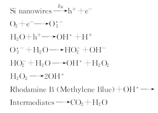
综上,我们提出了Mo-SiNWs形成的金属-半导体结构增强光催化性能的机理。图 5为Mo网衬底上生长的SiNWs产生电子-空穴对的示意图,有机染料的降解过程发生在SiNWs和Mo网构成的金属-半导体接触界面。由于费米能级的不同,SiNWs的能带在界面处会发生弯曲使得两者达到相同的位置,同时接触界面由于电荷积累而产生内势能,光激发产生光生载流子在内势能的作用下,电子-空穴对很容易分离其中,空穴到达SiNWs表面,捕捉水分子的电子生成 OH* 自由基团,而电子运动到Mo网衬底表面被氧气分子捕获而变为O·-2自由基团。随后,罗丹明B和甲基蓝染料易在这些活性自由基团的作用下形成中间产物,进而分解为无毒无污染的CO2 和H2O。有机物反应步骤如下所示[26, 27]:
 | 图4 不同染料的降解速率曲线 (a)罗丹明B;(b)甲基蓝Degradation rate curves of different dyes (a) Rhodamine B; (b) Methylene Blue |
 | 图5 SiNWs电子-空穴对产生机理示意图 Schematic of electron-hole generation in SiNWs on the Mo net substrate |
本文使用一步化学气相沉积法成功地在Mo网衬底上制备了大面积的呈垂直生长的SiNWs,其直径为5~30 nm,长度为1~30 μm。TEM表征发现获得的Si纳米线具有金刚石结构并沿着[001]方向生长,其表面覆盖了厚几个纳米的氧化层。利用获得的纳米线样品对罗丹明B和甲基蓝进行光降解测试,发现Mo-SiNWs这种金属-半导体结构具有优异的光催化能力,能快速降解以上有机染料,这表明直接在Mo网上合成SiNWS在光催化领域具有广泛的应用潜力。
| [1] | Smith R D L, Trudel S, Berlinguette C P. Photochemical route for the preparation of complex amorphous water oxidation catalyst[J]. In Emerging Materials and Processes for Energy Conversion and Storage, 2014, 58(45): 67-76. |
| [2] | Rettie A J E, Lee H C, Marshall L G, Lin J F, Capan C, Lindemuth J, McCloy J S, Zhou J S, Bard A J, Mullins C B. Combined charge carrier transport and photoelectroche-mical characterization of BiVO4 single crystals: intrinsic behavior of a complex metal oxide[J]. Journal of the American Chemical Society, 2013, 135(30): 11389-11396. |
| [3] | Wu W, Hao R, Liu F, Su X T, Hou Y L. Single-crystalline alpha-Fe2O3 nanostructures: controlled synthesis and high-index plane-enhanced photodegradation by visible light[J]. Journal of Materials Chemistry A, 2013, 1(23): 6888-6894. |
| [4] | Dong C S, Zhong M L, Huang T, Ma M X, Wortmann D, Brajdic M, Kelbassa I. Photodegradation of Methyl Orange under visible light by micro-nano hierarchical Cu2O structure fabricated by hybrid laser processing and chemical dealloying[J]. ACS Applied Materials & Interfaces, 2011, 3(11): 4332-4338. |
| [5] | Hamity M, Lema R H, Suchetti C A, Gsponer H E. UV-Vis photodegradation of dyes in the presence of colloidal Q-CdS[J]. Journal of Photochemistry and Photobiology A-Chemistry, 2008, 200 (2-3): 445-450. |
| [6] | Lo S C, Lin C F, Wu C H, Hsieh P H. Capability of coupled CdSe/TiO2 for photocatalytic degradation of 4-chlorophenol[J]. Journal of Hazardous Materials, 2004, 114(1-3): 183-190. |
| [7] | Konstantinou I K, Albanis T A. TiO2-assisted photocatalytic degradation of azo dyes in aqueous solution: kinetic and mechanistic investigations - a review[J]. Applied Catalysis B-Environmental, 2004, 49(1): 1-14. |
| [8] | Vinodgopal K, Kamat P V. Environmental photochemistry on surfaces - charge injection from excited fulvic-acid into semiconductor colloids[J]. Environmental Science & Technology, 1992, 26(10): 1963-1966. |
| [9] | Miller L W, Tejedor-Tejedor M I, Anderson M A. Titanium dioxide-coated silica waveguides for the photocatalytic oxidation of formic acid in water[J]. Environmental Science & Technology, 1999, 33(12): 2070-2075. |
| [10] | Gouvea C A K, Wypych F, Moraes S G, Duran N, Nagata N, Peralta-Zamora P. Semiconductor-assisted photocatalytic degradation of reactive dyes in aqueous solution[J]. Chemosphere, 2000, 40(4): 433-440. |
| [11] | Alexander B D, Kulesza P J, Rutkowska I, Solarska R, Augustynski J. Metal oxide photoanodes for solar hydrogen production[J]. Journal of Materials Chemistry, 2008, 18(20): 2298-2303. |
| [12] | Buda F, Kohanoff J, Parrinello M. Optical-properties of porous silicon - a 1st-principles study[J]. Physical Review Letters, 1992, 69(8): 1272-1275. |
| [13] | Shen M Y, Zhang S L. Band-gap of a silicon quantum-wire[J]. Physics Letters A, 1993, 176(3-4): 254-258. |
| [14] | Ma D D D, Lee C S, Au F C K, Tong S Y, Lee S T. Small-diameter silicon nanowire surfaces[J]. Science, 2003, 299(5614): 1874-1877. |
| [15] | Schoen D T, Schoen A P, Hu L B, Kim H S, Heilshorn S C, Cui Y. High speed water sterilization using one-dimensional nanostructures[J]. Nano Letters, 2010, 10(9): 3628-3632. |
| [16] | Schmidt V, Wittemann J V, Senz S, Gosele U. Silicon nanowires: a review on aspects of their growth and their electrical properties[J]. Advanced Materials, 2009, 21(25-26): 2681-2702. |
| [17] | Levine A, Yuan G B, Xie J, Wang D W. Preparations and energetic applications of Si nanowires[J]. Science of Advanced Materials, 2010, 2(4): 463-473. |
| [18] | Hochbaum A I, Yang P D. Semiconductor nanowires for energy conversion[J]. Chemical Reviews, 2010, 110(1): 527-546. |
| [19] | Schmidt V, Wittemann J V, Gosele U. Growth, thermodynamics, and electrical properties of silicon nanowires[J]. Chemical Reviews, 2010, 110(1): 361-388. |
| [20] | Mukherjee B, Smith Y R, Subramanian V. CdSe nanocrystal assemblies on anodized TiO2 nanotubes: optical, surface, and photoelectrochemical properties[J]. Journal of Physical Chemistry C, 2012, 116(29): 15175-15184. |
| [21] | Peng K Q, Wang X, Wu X L, Lee S T. Platinum nanoparticle decorated silicon nanowires for efficient solar energy conversion[J]. Nano Letters, 2009, 9(11): 3704-3709. |
| [22] | Huang X, Wang M, Willinger M G, Shao L, Su D S, Meng X M. Assembly of three-dimensional hetero-epitaxial ZnO/ZnS core/shell nanorod and single crystalline hollow ZnS nanotube arrays[J]. ACS Nano, 2012, 6(8): 7333-7339. |
| [23] | Chen Y W, Prange J D, Duehnen S, Park Y, Gunji M, Chidsey C E D, McIntyre P C. Atomic layer-deposited tunnel oxide stabilizes silicon photoanodes for water oxidation[J]. Nature Materials, 2011, 10(7): 539-544. |
| [24] | Dasgupta N P, Liu C, Andrews S, Prinz F B, Yang P. Atomic layer deposition of platinum catalysts on nanowire surfaces for photoelectrochemical water reduction[J]. Journal of the American Chemical Society, 2013, 135(35): 12932-12935. |
| [25] | Qu Y Q, Xue T, Zhong X, Lin Y C, Liao L, Choi J N, Duan X F. Heterointegration of Pt/Si/Ag nanowire photodiodes and their photocatalytic properties[J]. Advanced Functional Materials, 2010, 20(18): 3005-3011. |
| [26] | Huang X, Shang L, Chen S, Xia J, Qi X, Wang X, Zhang T, Meng X M. Type-Ⅱ ZnO nanorod-SnO2 nanoparticle heterostructures: characterization of structural, optical and photocatalytic properties[J]. Nanoscale, 2013, 5(9): 3828-3833. |
| [27] | Wang H, Wang J T, Ou X M, Li F, Zhang X H. Highly efficient and stable Si nanowires array embedded into transparent polymer for visible light photoelectrochemical cell[J]. Nanotechnology, 2014, 25(26): DOI 10.1088/0957-4484/25/26/265401. |